Overview
The 2006 ASUS A8M2N-LA HP Compaq OEM Desktop Motherboard is a microATX desktop computer motherboard produced by ASUS as an OEM system board for HP and Compaq desktop PCs. It belongs to the AMD Socket AM2 generation and represents a transitional mid-2000s desktop platform that combined DDR2 memory, PCI Express graphics expansion, SATA storage, legacy PATA/IDE storage, PCI expansion, and integrated NVIDIA graphics on one compact board.
The A8M2N-LA family appears under several OEM names and part-number variants. The board commonly associated with four DDR2 memory slots and four SATA connectors is often identified as the NodusM3-GL8E version. Other A8M2N-LA variants may have different memory-slot counts, SATA configurations, or rear I/O arrangements. For scrap identification, the visible board marking “A8M2N-LA” or “DABM2N-LA,” the Socket AM2 CPU socket, four long DDR2 DIMM slots, PCI Express x16 slot, NVIDIA BGA chipset package, and HP/Compaq OEM layout are the most useful identification features.
This motherboard is best classified as a desktop motherboard scrap board rather than a laptop, server, telecom, or industrial board. It is not a high-density gaming laptop board and does not contain a removable MXM graphics module. Its recycling value comes from the complete motherboard assembly, the CPU socket contacts, DDR2 memory slots, PCIe and PCI connectors, BGA chipset packages, copper inductors, MOSFET power circuitry, electrolytic capacitors, rear I/O connectors, SATA and IDE connectors, and the multilayer printed circuit board.
Basic Identification
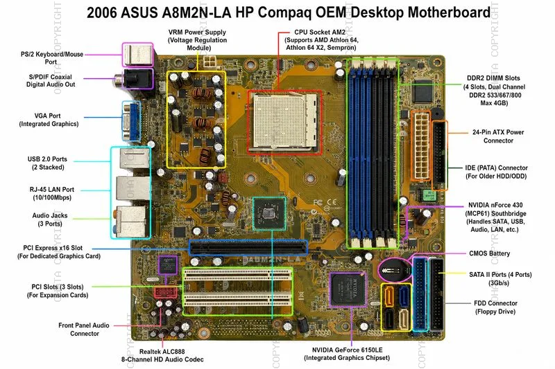
The ASUS A8M2N-LA is a square microATX desktop motherboard. The typical physical size is approximately 244 mm × 244 mm, equivalent to the standard 9.6 in × 9.6 in microATX form factor. The board uses a yellow-brown FR-4 PCB, a white Socket AM2 CPU socket near the upper middle section, four DDR2 DIMM slots to the right of the CPU socket, and a mixture of black PCI Express and white PCI expansion slots across the lower half.
2006 asus a8m2n la hp compaq oem desktop motherboard scrap identification Show All
The board in the reference image can be identified by the following visual features:
- White AMD Socket AM2 CPU socket
- Four DDR2 DIMM memory slots, usually arranged as blue and black pairs
- One black PCI Express x16 graphics slot
- Three white 32-bit PCI expansion slots
- NVIDIA BGA integrated graphics / northbridge chipset near the lower-middle area
- NVIDIA nForce 430 southbridge BGA chipset near the lower-right area
- Four SATA ports in orange, blue, black, and white
- One blue floppy connector and one black IDE/PATA connector near the right edge
- One 24-pin ATX main power connector and one 4-pin ATX12V CPU power connector
- Rear I/O cluster with PS/2, coaxial S/PDIF, VGA, USB, RJ-45 LAN, IEEE 1394 on some variants, and analog audio ports
The motherboard should not be confused with later DDR3 boards or Intel LGA boards. The Socket AM2 interface and DDR2 memory slots clearly place it in the AMD K8 desktop era.
CPU Socket and Processor Support
The A8M2N-LA uses AMD Socket AM2. Socket AM2 is a 940-pin organic micro pin grid array package interface. It is a PGA-style processor platform, meaning the processor package has pins and the motherboard socket contains receiving contacts. The socket uses a zero insertion force, or ZIF, lever mechanism, allowing the processor to be inserted without pressure and then locked into place.
The CPU interface type should therefore be identified as:
- CPU socket: AMD Socket AM2
- Contact style: PGA / micro-PGA
- Pin count: 940 pins
- Socket mechanism: ZIF lever socket
- Socket pitch: 1.27 mm
- CPU package size: approximately 40 mm × 40 mm, with the AMD package drawing showing a D/E body dimension range of 39.80 mm to 40.20 mm
This is important for scrap identification because Socket AM2 differs from Intel LGA sockets. In an LGA socket, the motherboard contains exposed spring pins and the CPU has flat pads. In this A8M2N-LA board, the CPU has the pins and the motherboard socket receives those pins. The gold-plated socket contacts and the removable CPU, if present, are important material-value indicators.
Supported processor families generally include AMD Athlon 64, AMD Athlon 64 X2, and AMD Sempron processors designed for Socket AM2. Common listings for the NodusM3-GL8E version identify support for Athlon 64, Athlon 64 X2, and Sempron processors, with a 2000 MT/s HyperTransport link. Some listings specify Athlon 64 X2 support up to 5000+, although exact processor compatibility may depend on BIOS revision and OEM configuration.
From a recycling perspective, the CPU socket area is one of the most important regions of the board. A complete board with the original CPU still installed normally has higher recovery and resale potential than a bare motherboard. A board with the CPU removed is still acceptable in many scrap streams, but it may be graded lower than a complete board. A board with the CPU socket damaged, cut out, burned, or chemically stripped is less desirable.
CPU Power Delivery and VRM Area
The CPU voltage regulator module is located around the CPU socket, mostly to the left and upper-left side of the socket. It contains copper inductors, MOSFETs, driver ICs, capacitors, and power traces. This VRM converts the 12 V input from the ATX12V connector into the low-voltage, high-current power rails required by AMD K8 processors.
Important VRM components include:
- Copper-wound inductors
- Aluminum electrolytic capacitors
- MOSFETs
- PWM controller ICs
- Ceramic capacitors
- Thick copper power traces
For scrap valuation, the VRM section contributes copper, aluminum, solder alloys, nickel, and semiconductor material. The visible copper coils are easy to identify and should not be removed unnecessarily if the board is being sold as complete motherboard scrap. Removing the inductors, capacitors, or MOSFETs may reduce the board’s grade because it makes the board appear stripped or processed.
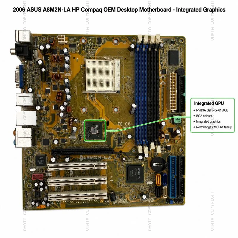
Chipset and Integrated Graphics
The A8M2N-LA is based on an NVIDIA GeForce 6150LE / nForce 430 chipset platform, although some documentation and board databases may describe related revisions as GeForce 6150SE / nForce 430 MCP61-family boards. The important point for scrap identification is that the board contains NVIDIA BGA chipset packages rather than a modern single-chip PCH or separate removable graphics card.
2006 asus a8m2n la hp compaq oem desktop motherboard scrap identification BGA Chiset
The integrated graphics function is associated with the NVIDIA GeForce 6150LE graphics chipset. This is an onboard integrated GPU design. It shares system memory rather than using dedicated graphics memory soldered onto the board. The rear VGA connector is the main visible output associated with this integrated graphics system. Some OEM variants also include S-Video or TV-out style connectors, depending on rear I/O configuration.
The integrated graphics chipset is a BGA package. BGA stands for ball grid array, meaning the chip is soldered directly to the PCB using solder balls underneath the package. For recycling, BGA graphics and chipset packages are important because they contain semiconductor die, copper, nickel, tin-based solder, and small amounts of precious-metal-bearing internal connections. However, the value is highest when the chip remains attached to the board. A motherboard with the integrated graphics chipset removed should be treated as incomplete and may be rejected or downgraded.
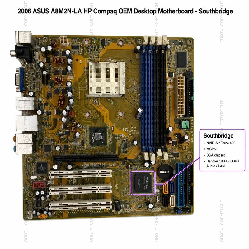
Southbridge / I/O Controller
The southbridge on the A8M2N-LA is commonly identified as NVIDIA nForce 430. It is located near the lower-right area of the board, close to the SATA connectors, IDE connector, CMOS battery, and front-panel headers. This chip handles many of the board’s lower-speed I/O functions.
The nForce 430 southbridge is responsible for functions such as:
- SATA storage interface
- USB 2.0 connectivity
- IDE/PATA interface
- Audio interface support
- LAN interface support
- PCI bus support
- System management functions
Like the integrated graphics chipset, the southbridge is a BGA semiconductor package. It is one of the most important scrap-value components on the board. Boards with the southbridge removed, chipped, cracked, burned, or heavily heat-damaged should be graded lower. A board missing this chip should not be treated as complete motherboard scrap.
Memory Support
The A8M2N-LA NodusM3-GL8E-style board uses DDR2 memory. The board in the reference image has four 240-pin DDR2 DIMM slots arranged in two color pairs, commonly blue and black. This color pairing indicates dual-channel memory support.
Typical memory specifications are:
- Memory type: DDR2 SDRAM
- Form factor: 240-pin desktop DIMM
- Channel mode: dual channel
- Supported speeds: DDR2-533, DDR2-667, and DDR2-800 on common NodusM3-GL8E listings
- Memory type requirement: non-ECC, unbuffered
- Maximum supported memory: commonly listed as 4 GB for HP/Compaq-approved configurations
The memory slots contain many gold-plated contacts. Even without memory modules installed, the slots contribute to the board’s recovery value. If DDR2 memory modules remain installed, they should normally be removed and sorted separately because memory modules are a separate recoverable category with their own gold-plated edge connectors and DRAM ICs.
For grading, complete and undamaged memory slots are preferred. Broken clips, cracked slot housings, missing slots, or heavy corrosion can reduce the board’s value.
Graphics Expansion
In addition to onboard integrated graphics, the A8M2N-LA provides one PCI Express x16 slot for a dedicated graphics card. This long black slot is located below the integrated graphics chipset area and above the three white PCI slots.
2006 asus a8m2n la hp compaq oem desktop motherboard scrap identification GPU NVIDIA GeForce
The PCIe x16 slot should be identified as:
- Graphics expansion interface: PCI Express x16
- Purpose: dedicated graphics card installation
- Physical slot color: usually black
- Scrap value feature: gold-plated internal contacts
This board does not contain a removable laptop-style GPU module. There is no MXM slot and no separate video memory array around a discrete GPU. Therefore, when identifying the GPU area for scrap purposes, the relevant graphics component is the onboard NVIDIA GeForce 6150LE integrated BGA chipset plus the PCI Express x16 slot for optional add-in graphics.
Storage Interfaces
The A8M2N-LA includes both modern-for-its-era SATA storage and legacy IDE/PATA support. The board shown has four SATA ports near the lower-right area. These are typically color-coded and mounted near the southbridge. Many listings describe the NodusM3-GL8E version as having four SATA connectors, with SATA II / 3.0 Gb/s support in common specifications. Some other A8M2N-LA references list SATA 1.5 Gb/s for certain part-number variants, so lot identification should consider the exact OEM revision.
The board also includes a large black 40-pin IDE/PATA connector. This connector supports older parallel ATA hard drives or optical drives. It contains many metal contacts and is visually important for identifying the board as a mid-2000s transitional motherboard.
A blue floppy drive connector is also visible near the right edge. The floppy connector has low standalone value but confirms the board’s generation and legacy desktop design.
Storage-related visible features include:
- Four SATA ports
- One IDE/PATA connector
- One floppy drive connector
- Southbridge chipset located nearby
- Front-panel and internal USB headers close to the lower-right edge
Expansion Slots
The board provides a mixed expansion layout:
- One PCI Express x16 slot
- Three 32-bit PCI slots
The PCI Express x16 slot was intended for graphics expansion. The three PCI slots were intended for sound cards, network cards, modem cards, capture cards, USB expansion cards, or other legacy peripherals.
From a recycling perspective, expansion slots contain plastic housings, plated contacts, solder, and copper connections to the PCB. They are not usually removed one by one unless processing large quantities, but intact expansion slots help maintain the board’s grade. Missing PCI or PCIe slots indicate stripping and may reduce value.
Rear I/O Ports
The rear I/O section is located along the left edge of the motherboard. Depending on exact revision, it may include:
- PS/2 keyboard connector
- PS/2 mouse connector
- Coaxial S/PDIF digital audio output
- VGA output for integrated graphics
- USB 2.0 ports
- RJ-45 Ethernet port
- IEEE 1394 / FireWire port on some variants
- Analog audio jacks
- Possible S-Video output on some OEM versions
These connectors contain copper, steel, nickel plating, and small amounts of gold or other plated contact material. The RJ-45 Ethernet jack, USB ports, VGA connector, and audio jacks are all visible scrap-value contributors, although their individual value is lower than CPU, GPU/chipset, and memory-related components.
Rear I/O ports should usually remain attached when grading complete motherboard scrap. Removing them may reduce board completeness and make visual identification harder.
Audio and Network Components
Common A8M2N-LA listings identify Realtek ALC888 or similar high-definition audio codec support, depending on the exact board revision and source. The audio codec is a small IC near the rear audio area and internal front-audio header. It supports multichannel HD audio output in OEM desktop configurations.
Network support is commonly listed as 10/100 Ethernet on many A8M2N-LA references, with Marvell or Realtek physical-layer components depending on revision. Some reseller listings may describe different network capabilities, so the exact controller should be confirmed from the chip marking when possible. For scrap identification, the network IC, RJ-45 jack, and associated magnetics are modest but recognizable value contributors.
BIOS, CMOS Battery, and Firmware Area
The motherboard includes a BIOS/flash ROM chip, typically a small rectangular IC used to store firmware. The CMOS coin-cell battery holder is located near the lower-right area. The battery powers CMOS settings when the computer is unplugged.
For shipment and recycling preparation, coin-cell batteries should be handled according to battery recycling rules. The battery holder itself can remain on the board, but loose or damaged batteries should not be mixed with clean motherboard scrap. Battery leakage, corrosion, or acid damage can reduce board value.
Power Connectors
The A8M2N-LA uses a standard 24-pin ATX main power connector and a 4-pin ATX12V CPU power connector. The 24-pin connector is located near the right side of the board, next to the memory area and IDE connector. The 4-pin CPU power connector is located near the upper-left side of the CPU socket and VRM area.
These connectors are important identification points because they confirm that the board is a standard desktop ATX-family motherboard rather than a proprietary laptop board. They also contain copper alloy contacts and soldered through-hole joints.
Scrap Value Classification
The ASUS A8M2N-LA should generally be considered a mid-grade desktop motherboard scrap item when complete. It is more valuable than low-grade appliance control boards but normally less valuable than server boards, telecom boards, or gaming laptop boards with dedicated high-density GPU circuitry.
Its value is supported by:
- Socket AM2 CPU socket with gold-plated contacts
- Possible removable AMD CPU
- DDR2 memory slots with plated contacts
- PCI Express x16 slot
- Three PCI slots
- NVIDIA BGA integrated graphics chipset
- NVIDIA nForce 430 southbridge chipset
- Copper VRM inductors
- MOSFET and capacitor power circuitry
- SATA, IDE, USB, LAN, VGA, and audio connectors
- Multilayer copper PCB
The board is not a premium modern motherboard, but it remains a recognizable desktop motherboard scrap category due to its complete CPU socket, multiple connector types, and two major BGA chipset packages.
Accepted Material Condition
A complete A8M2N-LA motherboard scrap unit should ideally include:
- Intact PCB
- CPU socket present
- NVIDIA integrated graphics chipset present
- NVIDIA southbridge chipset present
- DDR2 DIMM slots present
- PCIe and PCI slots present
- SATA, IDE, and power connectors present
- Rear I/O ports present
- VRM components present
- No excessive plastic or unrelated mixed waste
- No severe burn damage or liquid corrosion
The best scrap condition is a clean, dry, uncut, unstripped board with original components still attached. If the CPU and RAM are installed, they should be evaluated separately or identified as attached value items.
Not Accepted or Downgraded Conditions
The following conditions may cause rejection or downgrade:
- Removed NVIDIA BGA chipset packages
- Removed integrated graphics chipset
- Removed southbridge chipset
- Cut-out CPU socket
- Missing memory slots
- Missing PCIe or PCI slots
- Heavy stripping of copper coils, MOSFETs, or connectors
- Broken PCB sections
- Burned or charred board areas
- Water damage or corrosion
- Oil contamination
- Mixed garbage, plastic housings, or non-electronic waste attached
- Loose batteries mixed with the board lot
- Boards with hazardous contamination
For this specific model, the integrated graphics chipset and southbridge chipset should not be removed. A board missing these BGA chips is no longer a complete motherboard scrap item and should be graded lower or rejected depending on buyer standards.
Preparation Tips for Recycling
To preserve the best scrap value:
- Keep the board dry and clean
- Do not cut the board
- Do not remove BGA chipset ICs
- Do not strip the CPU socket
- Remove loose batteries if required by the buyer
- Separate RAM modules if sold as memory scrap
- Keep desktop motherboards separate from laptop boards, power supply boards, and low-grade appliance boards
- Avoid mixing with cables, plastic bezels, fans, steel brackets, and non-board materials
- Package boards flat to prevent cracked PCB corners and broken slots
The most important rule is to preserve component completeness. A complete, identifiable A8M2N-LA motherboard is easier to grade and more desirable than a partially harvested board.
Component-Level Recovery Notes
Although this board can be processed as a complete motherboard, component-level recovery may separate material streams such as:
- CPUs
- RAM modules
- BGA chipset packages
- Gold-plated connectors
- Copper inductors
- Aluminum capacitors
- Steel shields
- PCB base material
However, component-level dismantling should be done only by qualified recyclers or specialized processors. For ordinary suppliers, unnecessary removal of components often lowers board grade. A board that has been stripped of chipset ICs, slots, sockets, or connectors may lose more value than the recovered parts are worth.
Summary
The 2006 ASUS A8M2N-LA HP Compaq OEM Desktop Motherboard is a mid-2000s AMD Socket AM2 microATX desktop board using DDR2 memory, NVIDIA integrated graphics, NVIDIA nForce 430 southbridge functions, PCI Express x16 graphics expansion, PCI legacy expansion, SATA storage, IDE/PATA storage, USB 2.0, Ethernet, audio, and standard ATX power input.
For technical identification, the most important confirmed features are the Socket AM2 PGA/ZIF CPU socket, approximately 40 mm × 40 mm AMD processor package size, DDR2 DIMM memory slots, PCIe x16 graphics slot, NVIDIA BGA chipset packages, and four SATA/legacy IDE storage layout. For scrap identification, its value depends strongly on completeness. The CPU socket, chipset ICs, memory slots, expansion slots, gold-plated contacts, copper VRM coils, and multilayer PCB should remain intact whenever possible.
A complete A8M2N-LA board should be treated as desktop motherboard scrap with moderate recovery value. Boards with removed chipset ICs, missing CPU sockets, broken memory slots, cut PCB sections, corrosion, burn damage, or heavy stripping should be downgraded or rejected.